Prologue
This is a series of tutorials on how to code on Xilinx FPGAs using the Vivado Design Suite. At the start of each tutorial, I will be mentioning the board I used. However, if you smartly use this text, I am positive that you will be able to use it for other boards as well. In case I miss some information, I will be reading the comments and will try to incorporate them into my text.
Before you guys start reading this tutorial, here is some information about me. I am a Ph.D. student who has recently started coding in hardware and FPGAs and would like to share the knowledge as it has been exhausting and overwhelming for me to understand how FPGAs work, not because it is difficult, but because the text is spread out all over the internet without a structure, and wherever you happen to find it, it is not explained in a simplistic manner. So this tutorial is for a very targeted audience who are starting to code with Xilinx FPGAs using Vivado. In case, I miss something or I fail to explain or illustrate something, I will appreciate constructive feedback. One last thing before we jump to the tutorial, this is not a how-to-learn Verilog blog. I might write that one in the future. However, when I was learning there were two sites that really helped me:
The tutorial starts now …
The Beautiful Lights
Note: This tutorial will not cover the installation procedure for Vivado. However, one thing that I missed while installing Vivado was if you are using a Linux distribution, you have to install the cable drivers separately after installing the suite otherwise your hardware manager would not detect your FPGA.
Hardware and software specs used:
Vivado: 2018.1
OS: Ubuntu 18.04
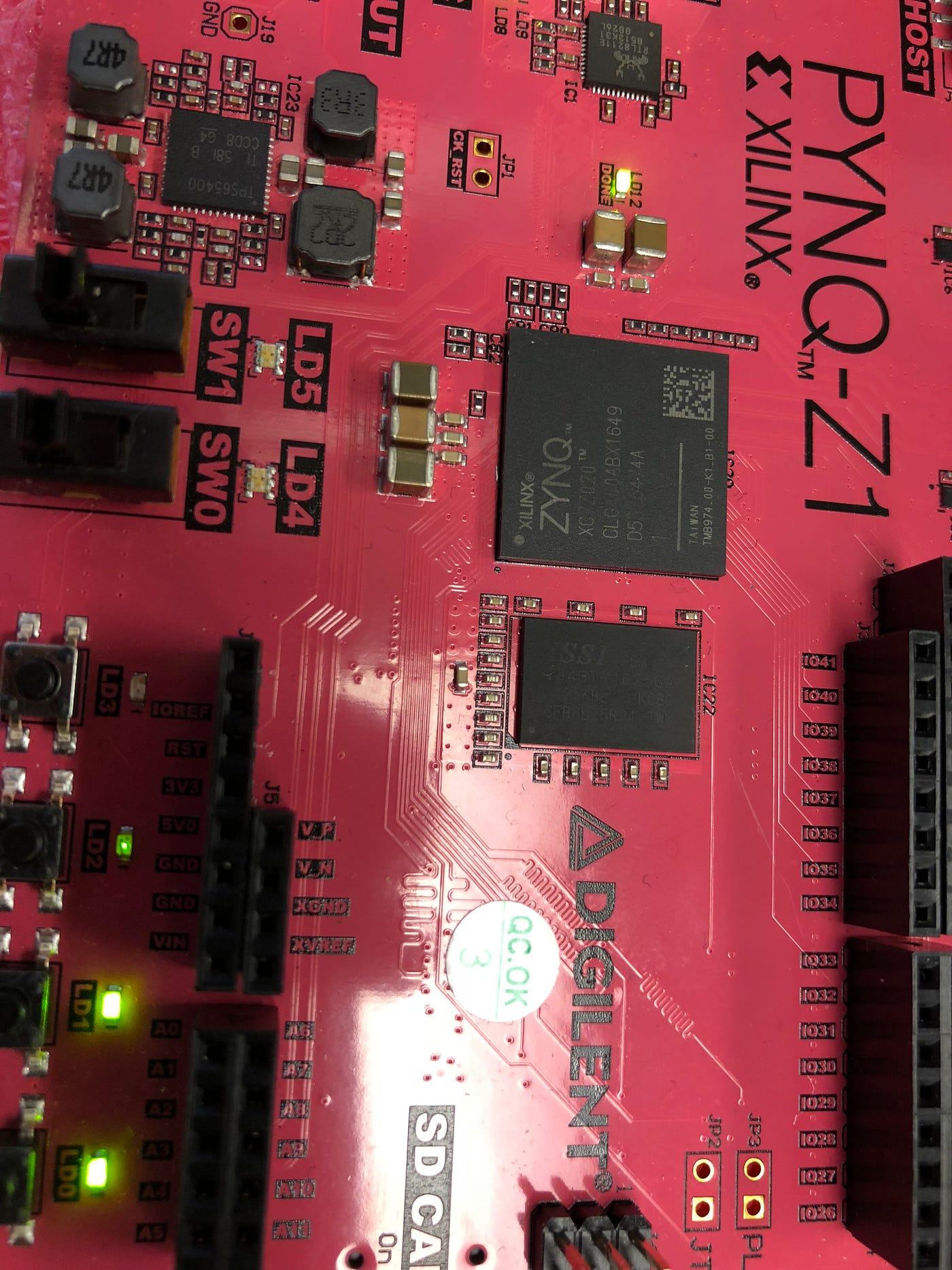
Board: PYNQ-Z1

This will be the very first project you will build on an FPGA(the And gate does not count which you started off with while learning Verilog / VHDL).
Step 1: Create project
Create Project -> Next -> Give the project name -> RTL Project (Check do not specify sources at this time) -> Select your board (in my case it is Pynq-Z1) -> Finish


Step 2: Write the code
Add “Design Source” i.e. your verilog code to blink the light. There is a little bit of math involved in why we do what we do in this code. I’ll explain that eventually. Firstly, let’s add it.
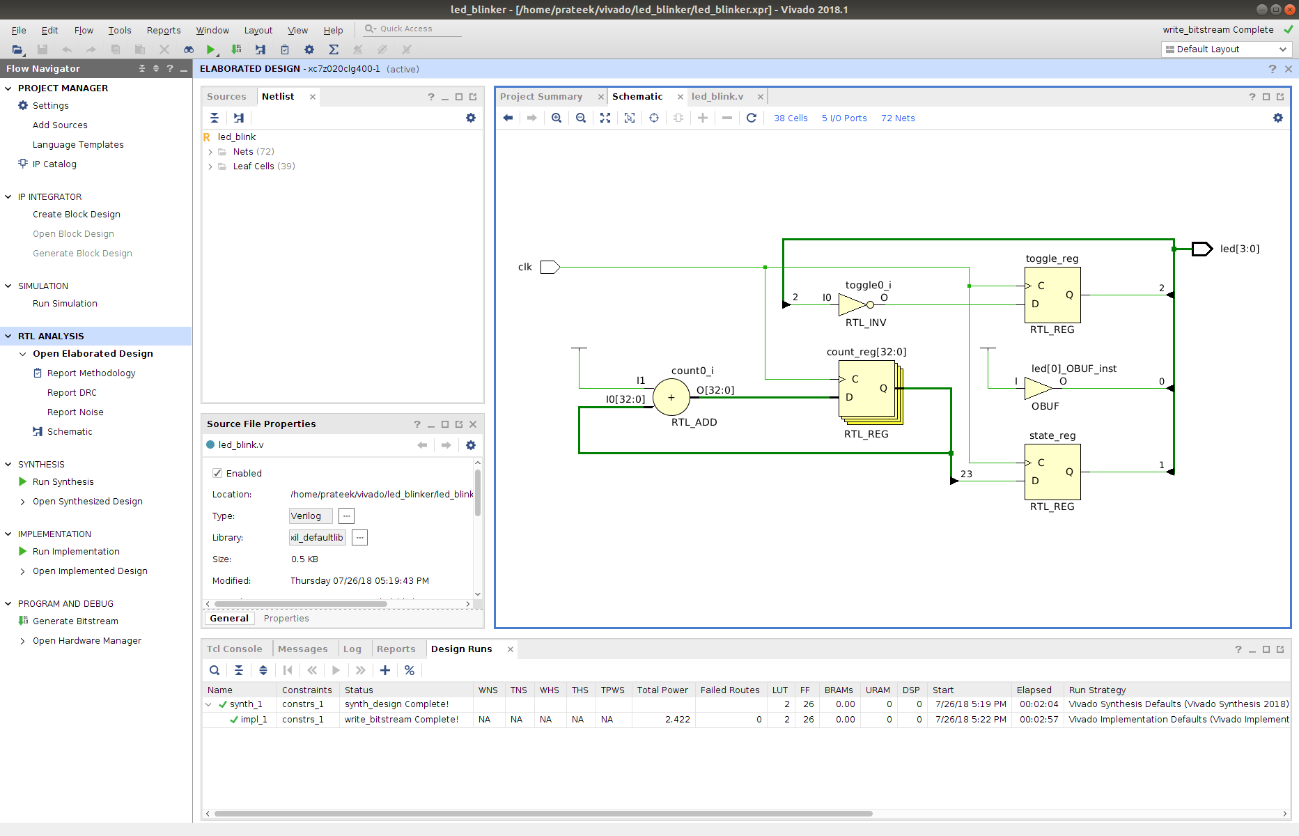
The left most side bar is called the flow navigator.

Some brief information about the Flow Navigator:
It specifies the basic flow of Vivado. The first links are of project manager. It lets you add sources, constraint files etc. Then comes IP integrator which lets you create block design. With the help of block designs you can make complicated architectures without even writing the verilog code from scratch. After writing the code, usually people simulate their code which basically is a quick debug strategy. You have to write a testbench to do that which is not part of this tutorial but I can include it later on for a bit complicated designs. Simulation is not a mandatory step but it is considered to be a good practice as the testing the code on the board takes a lot of time. Even the slightest change in the code may take 10–15 min to synthesize on the board.
Simulation is followed by synthesis, implementation and generation of bitstream. This bitstream is transferred to the board which basically runs the code. You can do all these steps one by one or you can do these steps directly by clicking generate bitstream and vivado handles synthesis and implementation automatically. I did not mention simulation as it is not a mandatory step and is just for the programmer to do it for debugging. I’ll show you the shortest way where we will click to generate the bitstream and vivado will handle the simulation and the implimentation.
Coming back to the step 2:
Writing the verilog code..
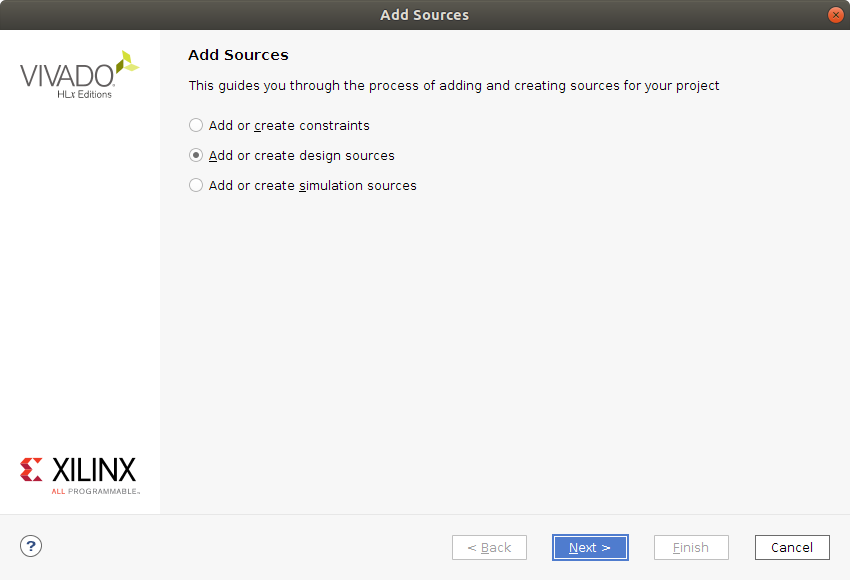
Go to “Add Sources” in the flow navigator -> Add or create design sources -> create file -> give the filename : “led_blink” in this case. A define module window will open, you can just click OK again followed by a Yes for a reconfirmation.


Now, replace the existing code with the following:`timescale 1ns / 1psmodule led_blink(
input clk,
output [3:0] led
);
// led 0
reg data = 1'b1;
reg [32:0] counter;
reg [32:0] count;
reg state;
reg toggle;assign led[0] = data; // static value of led
assign led[1] = state; // blinker
assign led[2] = toggle; // 50% brightness
always @ (posedge clk)
begin
counter <= counter + 1;
count <= count + 1;//led 0
state <= count[23];//led 2
toggle <= ~toggle;
endendmodule
Step 3: Assign the pins
Before we start the synthesis we need to assign physical pins to the input and output ports.
To assign the port we need to first check what are the physical pins. Since, the board I am using is a pynq board. Therefore, I will have to check the pin specifications in the circuit diagram given in the reference manual(https://reference.digilentinc.com/reference/programmable-logic/pynq-z1/reference-manual).
In the following figure you can see that the clock is H16 and the LEDs are R14, P14, N16 and M14 respectively.


Go to “Open Elaborated Design” on the flow navigator. A schematic page will be opened.

Click on “5 I/O Ports” right below the tab name which says schematic. This will open a tab on the bottom window titled “Find Results”. Set all the package pins

Save the pins by hitting Ctrl+s. A window will pop up where you have to save the constraint file.

Step 5: Generate Bitstream
Go to generate bitstream at the bottom of the flow navigator.

Select View Reports and then click OK.
Step 6: Program the FPGA
Connect the FPGA in the Jtag mode using the USB cable. Open Hardware Manager. Click Open target -> Auto connect -> Program device -> Program.


That should get your LEDs blinking!
Just a spoiler for the next part — there is a reason why the lights are called beautiful… the next episode, lights might be a bit ugly.
Happy Learning!
